Sunday Brief – Nov 9, 2025
Another solid week across the @TatsuEcosystem . We closed one loop, opened another, and kept the rails steady for builders.
Brief Summary
Challenge 0009 launched successfully, targeting higher performance and lower area over the design finalized in…
ChipForge: Challenge_0009 — Refining the RV32IMCK Core 🔧
We’re entering the optimization phase! After adding RISC-V crypto support, this round focuses on making the RV32IMCK core faster and more efficient.
Starting from the provided reference (Challenge_0008_Solution.zip),…
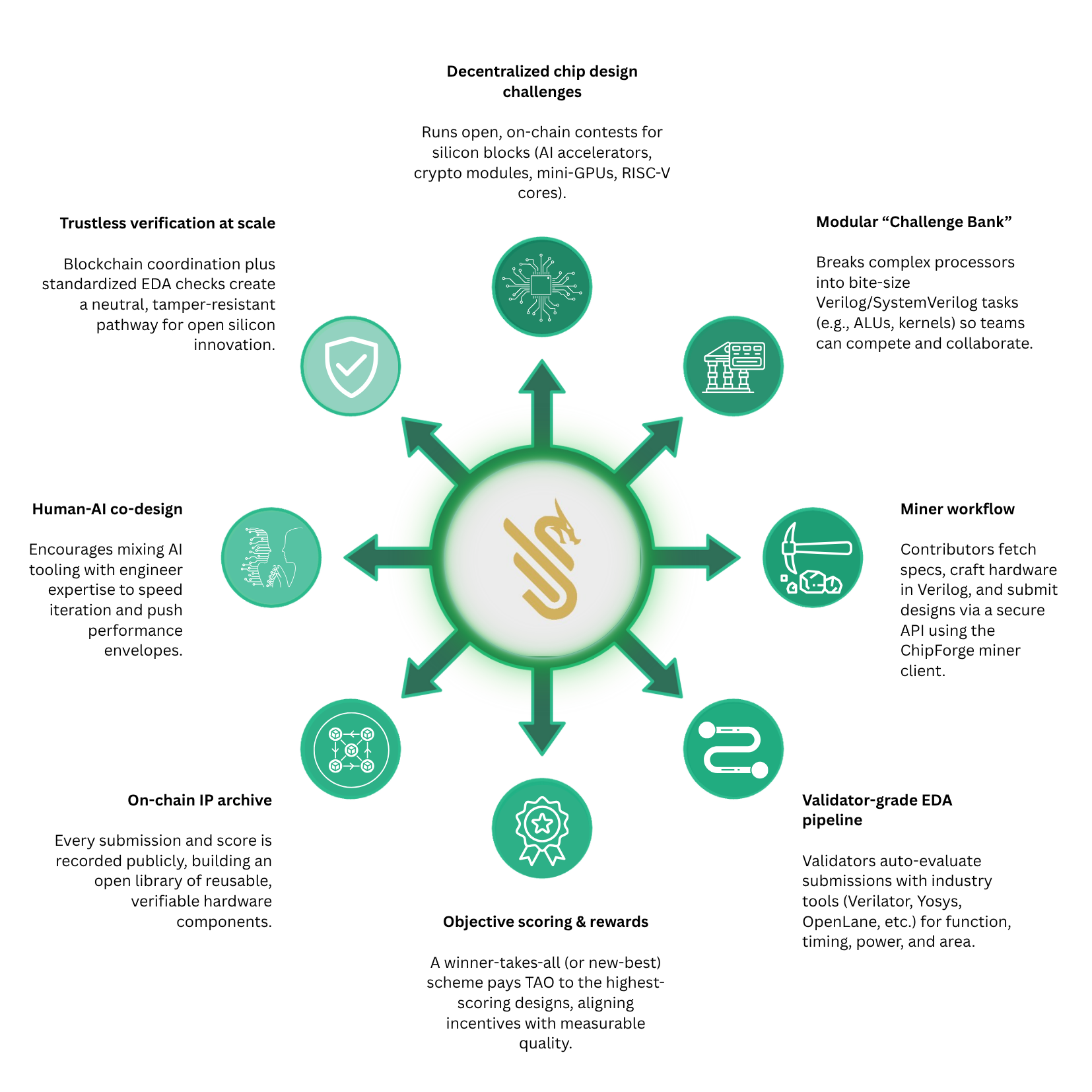
The ChipForge (SN84) Whitepaper Is Now Live!
Today marks a historic milestone—the official release of the ChipForge (SN84) Whitepaper, the foundation of the world’s first decentralized chip design project.
The whitepaper explores how ChipForge integrates blockchain, AI, and…
Sunday Brief – Nov 2, 2025
Dear TATSU Community, this week we strengthened our infrastructure while preparing for the next phase of hardware design challenges.
Challenge Wrap-Up & Next Steps
Challenge_0008 (RV32IMCK) closes tomorrow with the leading solution achieving 100%…
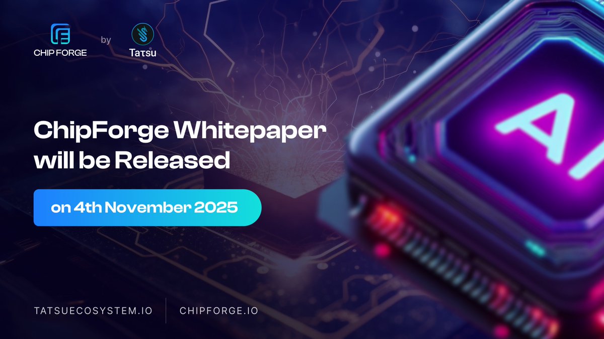
ChipForge (SN84) Whitepaper Release Date Confirmed
We’re thrilled to announce that the ChipForge (SN84) Whitepaper will be officially released on November 4, 2025.
As the first decentralized chip design project not only on @bittensor but whole Web3 Space, ChipForge is pioneering…
http://x.com/i/article/1983874830471507968